Chip Scale Thermal Pad: Thermal Management for 16-Hi HBM and Co-Packaged Optics
Discover how OIP Technology’s direct sintered metal thermal pad eliminates critical hotspots and unlocks sustained performance for high-power logic, HBM stacks, and optical modules.
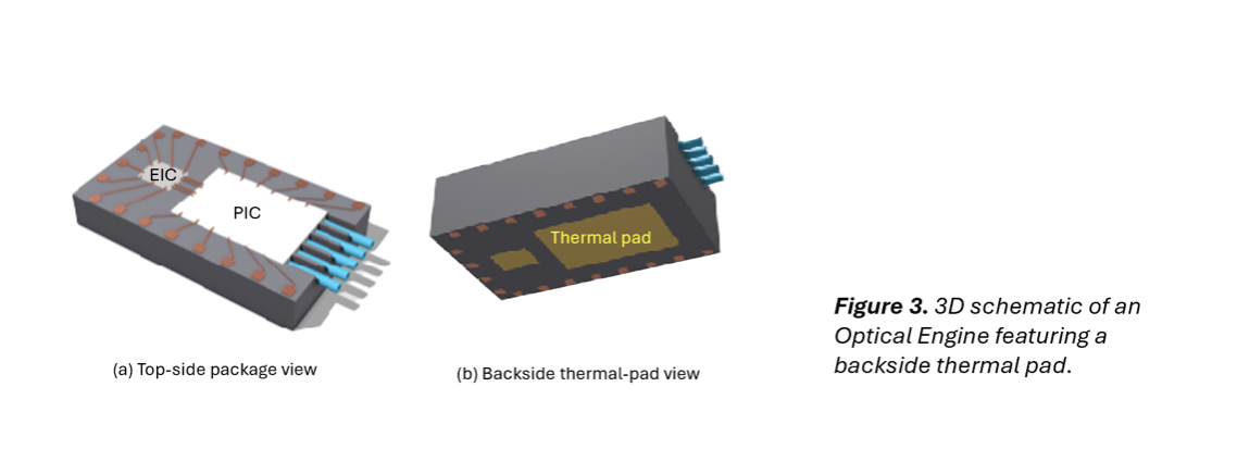
Our advanced sintering technology enhances heat dissipation for high-performance AI/HPC Logic, HBM, HBF, and Next-Gen optical modules.
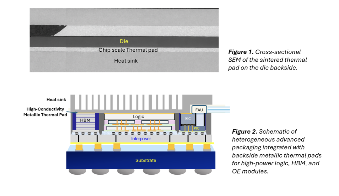
As artificial intelligence (AI), high-performance computing (HPC) drive chip power densities to unprecedented levels, thermal dissipation has become the primary bottleneck in next-generation semiconductor packaging. To address this critical challenge, OIP Technology has developed a Backside Thermal Pad Technology featuring advanced high-conductivity metal sintering directly on the die backside.
Designed to replace conventional high-thermal-resistance TIMs (Thermal Interface Materials), this proprietary backside thermal pad establishes a sintered metallurgical bond with the silicon substrate. By maximizing interfacial contact area and minimizing thermal boundary resistance, the technology delivers exceptional heat-spreading performance directly from the junction to the heat sink.