

Advanced Packaging Solutions:
Optical · Intelligence · Power
Optical module: ultra thin optical module (0.15mm thick) for mobile and wearable devices
AI Optics: CPO, Optical I/O
Power package: Advanced packaging with low power consumption.

Experts in optical interconnect leveraging CPO
We are a semiconductor advanced packaging firm focused on manufacturing and custom design for the world’s leading technology innovators and companies.


OIP TECHNOLOGY
OIP TECHNOLOGY
-
Silicon photonics module with edge coupling and top coupling.
Ultra-thin VCSEL module package.
Chip scale thermal pad.
3D stack chiplet for optical and high power applications.
3rd generation FOPLP with integrated optics and chips.
Patented Thin Mini-LED Display.
Integrated solar panel module.
-
AI
Photonics module(Transceiver and Data center co-packages)
AI optics pluggable FAU (for AI GPU)
Consumer
VCSEL sensor
CIS module
Energy
Integrated solar
Flexible package
Automotive
Lidar sensor
High Power packages (Hybrid TO, BSM, Two-sided metal packages)
Chip scale atomic clock
-
Semiconductor assembly.
Panel level test.
Research and Development
-
High frequency product
Good heat dissipation.
Optical package thickness reduction.
-
We provide custom design, manufacturing and project services to the world’s leading technology companies. Connect with us to learn more.

AI / HPC
-
Top coupling
Edge coupling
Chip scale thermal pad
-
Connect fibre optics to chip
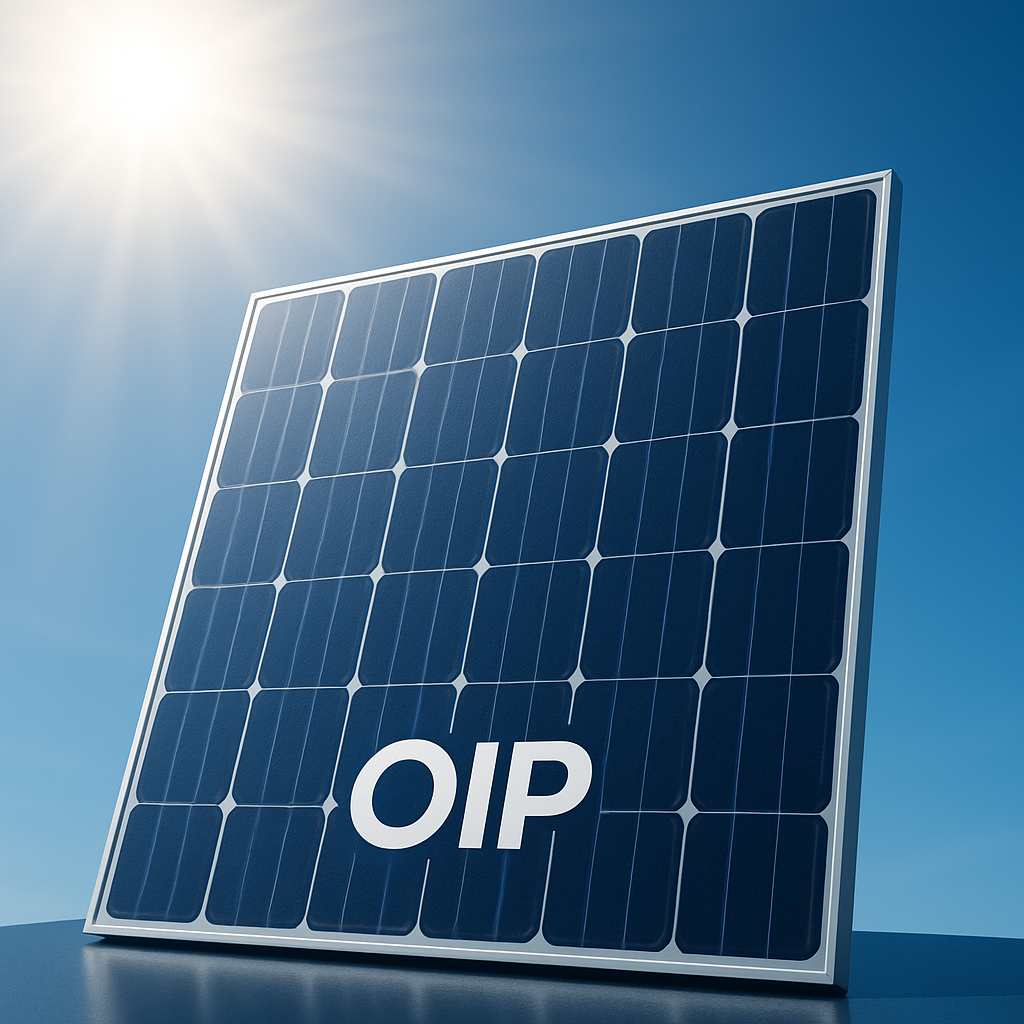
Renewable Energy
-
Low light applications.
Low power consumption with Integrated chip.
100% light absorption design.
Narrow die gap at 10um

Consumer
-
Ultra-thin package at 0.2mm for wearable devices.
-
Integrated driver IC and LED.
Single pixel control.
Excellent thermal performance.
Low CTE mismatch
-
New EMC material enable 180 degree bending.

Automotive
-
. Applicable for Lidar module
. Large metal post for high current.
. Excellent thermal dissipations,
-
. Thick metal RDL.
. 2-side metal exposed.
Contact Us
Interested in working together? Fill out some info and we will be in touch shortly. We look forward to innovating together.