

Optical Packaging Solutions: CPO, Optical I/O and Laser Diode Array
-

Co-Packaged Optics Platform
Silicon photonics-based CPO
Supports both top and edge coupling
Chip-scale thermal pad on the die backside
-
Optical I/O (Top Coupling)
Enables fiber-optic connection to the top surface of the photonic chip.
Pluggable optical I/O
Reflow-compatible optical I/O
-
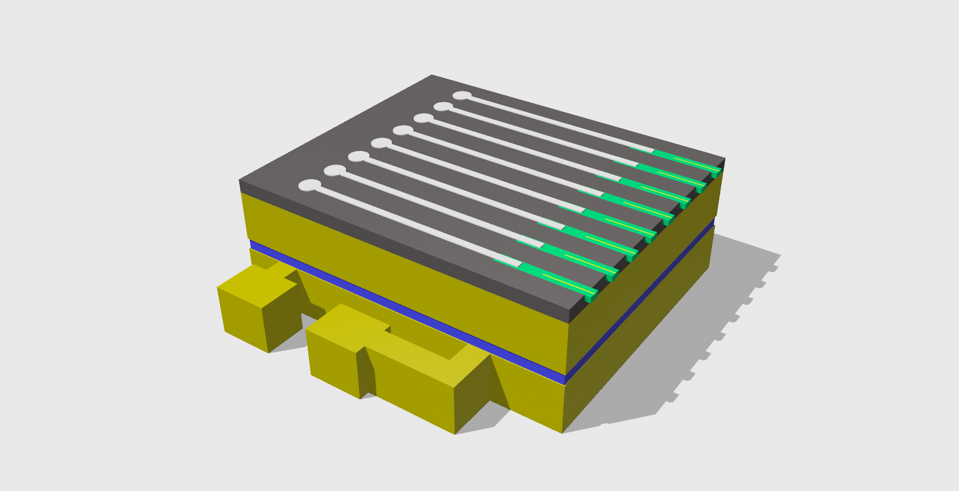
Edge-Emitting Laser Module
Modular design enables fiber-optic coupling
Excellent BLT and die-tilt control
Reduces optical coupling and alignment time by up to 80%
±5 μm die-placement accuracy
Excellent thermal dissipation design.
-

3D uLED Package
Driver and LED integration.
Low cost 3D structure.
FOPLP process.